


图表内容
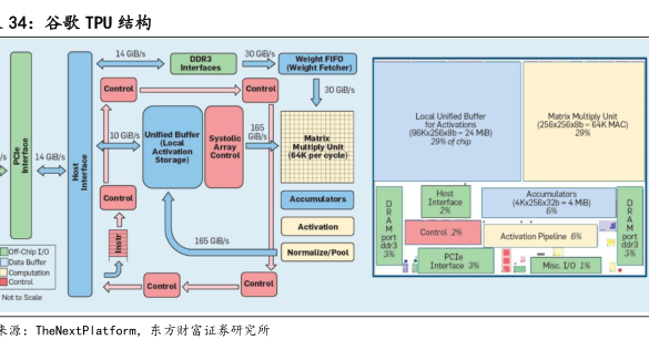
34:谷歌TPU结构
14 GiB/s
30GB/s
DDR3
Welght FIFO
Contro
30 GiB/s
96K0256x8b-24MB
Systolle
Activation
Array
5 torage】
Control
Host
4K255x32西=4MB
Activation
165G8
Activation Pipeline 6%
of-chip L/O
Normalize/Pool
PCIe
Control
源:
TheNextPlatform
东方财富证券研究所

